Backstory
So it was the end of the year again and everything got decorated for christmas. This time I got an extra job to “make the illumination of the crib properly”. Great, I had some cool COB LED strips waiting for a proper use case, whose time now came.

To make it more of a warm / candle light, I covered parts of the strip with kapton tape, making it more yellowish, which fits the purpuse of lighting an old shed with straw and animals.
However the light was quite bright and I was missing some candle-like flickering, so I quickly designed a ESP32-C6 board as I wanted to play with it’s Zigbee capabilities anyway and implement a Zigbee controlled crib, varying brightness and flicker mode.
The LED-strip required 12V, so I needed a USB PD chip to trigger the power supply to deliver this voltage. Then some el cheapo MOSFETs and a mini screw terminal, done.
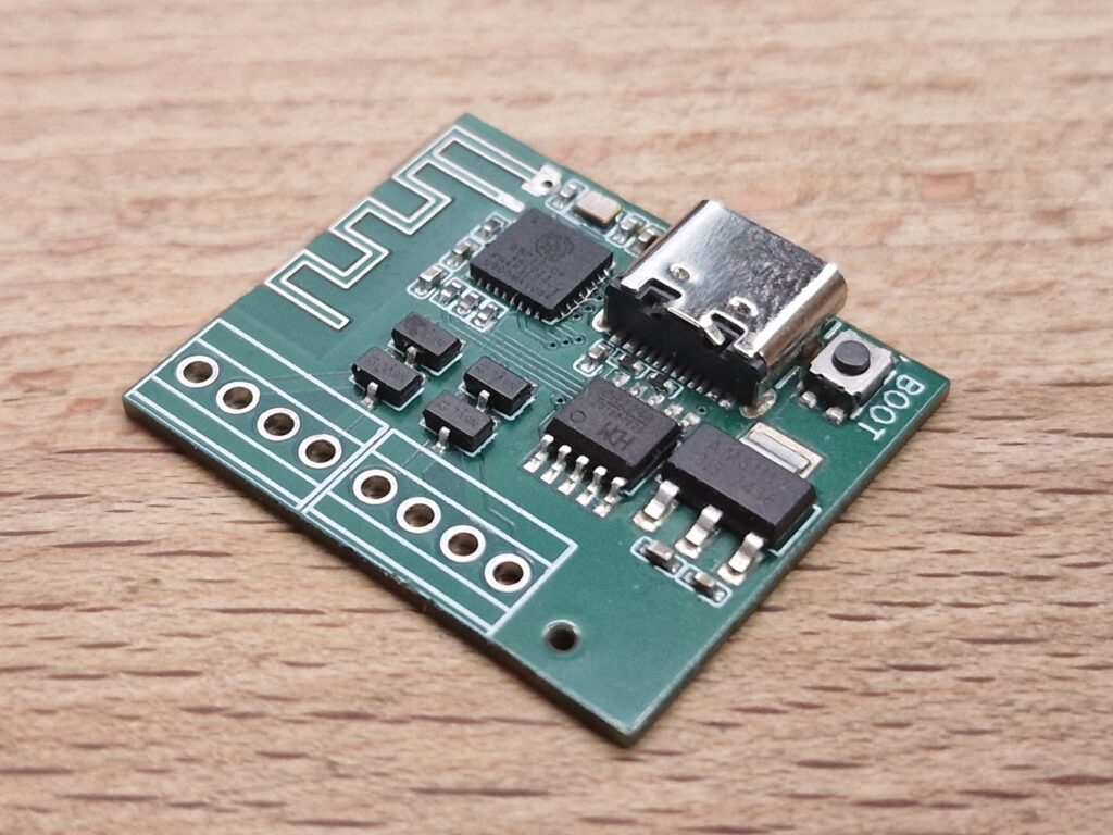
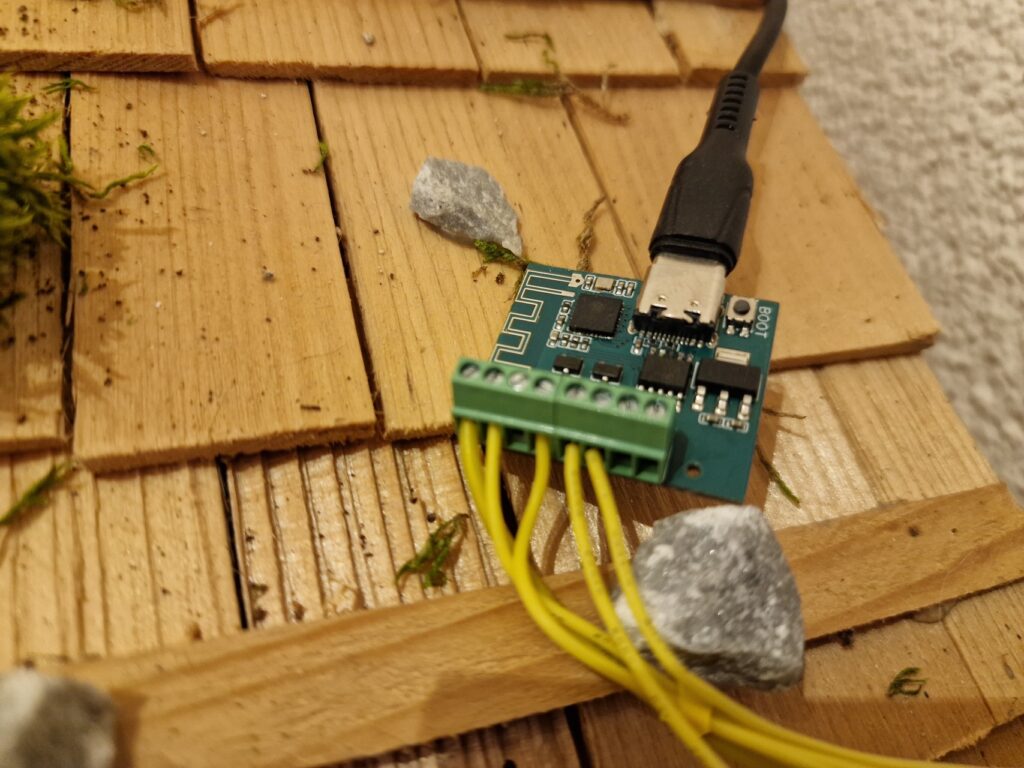
You probably notice the AMS1117, which is not very suitable for powering an ESP32 from 12V. Absolutely correct – however I hoped that the Zigbee peripheral allows the CPU to sleep all the time, waking it up only when it has to do something. Unfortunately this is not possible, so either the CPU is running all the time, handling all the protocol stuff or you “disconnect” from the mesh and wake up and “connect” again, causing a huge delay in processing on/off commands.
This ended up with the AMS getting a bit warm. Not desastrous hot, but beyond common design targets. Okay, next time maybe the MPM3620, which unfortunately isn’t available on lcsc.com.
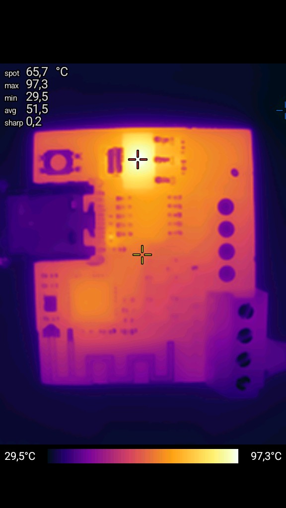
Implementing all the possible power savings, you can pull out of an ESP32-C6 (while still having Zigbee active), the AMS now has somewhere around 50°C. This is okay, as this was a quick prototype for experimenting with Zigbee while practically serving a purpose in the crib.
A second PCB now powers my desktop light – also a COB strip above my desk, that lights up my wall and my desk without blinding me.
USB-PD Trigger Chip
As you can see on the pictures, I am using an USB C plug and a CH224K to tickle 12V out of the USB PD power supply. And this chip in its SOIC-8 footprint is as big as the ESP32-C6 itself. While usually this is not much of a problem, sometimes you want to save precious PCB space.
So the question arose – why not bitbang PD-protocol with the ESP32 and save precious PCB space?
Is this even possible? Or can we use a peripheral for this task?
Is it possible for the ESP32 to speak USB-PD?
Good question. Is it?
Googling around doesn’t answer this question immediately. Could not find a project that does *not* use a CH224 or alike to trigger USB PD. Neither google nor github revealed that there was something like that around on the interwebs.
Noone seems to use the ESP32 itself to trigger PD.
There are a few articles going into depth of the PD protcol, however just for decoding. But they give a good impression of what to expect when listening to the bus.
(however I still wonder why his first approach to a level shifter would work at all :) )
Lets find out ourselves.
Electrically
For the source to detect a sink, the most obvious thing is the 5.1k pulldown. This is quite straight forward. Maybe we can emulate this through the ESPs pulldowns or weak driving to ground, but maybe we should there just follow the specification. At least this one little thing.
The Rx/Tx voltages leave much more room for violating standards. Lets check those.
Checking the “USB_PD_R3_2 V1.1” named USB PD spec version v1.1 reveals the low voltage for Tx must be 0V and the high voltage in a window of 1.0V-1.2V. The acceptance (Rx) mask is much more relaxed, down to 0.8V-1.2V depending on the sourcing state of the supply.
The more current the sink draws, the higher the voltage drop on ground and the window narrows. So the transceivers have to have quite large tolerance bands, which is good for us.
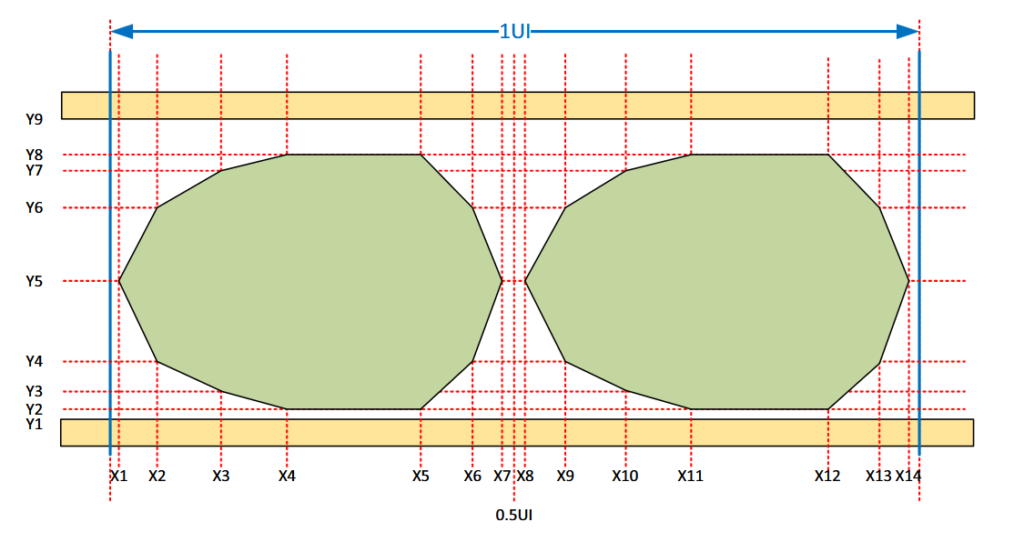
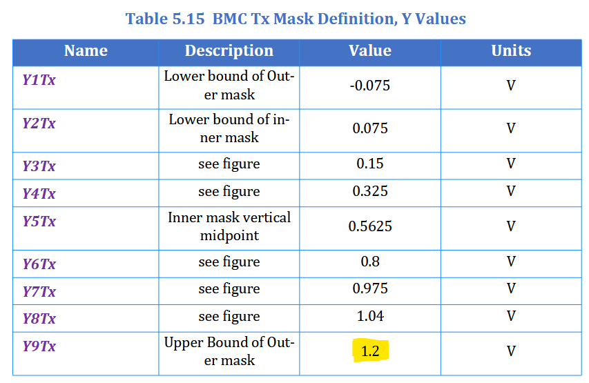
However this is outside all GPIO specs and the ESP32 would never detect any high level.
Using the ADC would be an option, but the ADC peripheral doesn’t have some alerts that can be triggered when a sample is above/below certain ADC count values.
Microcontrollers like the Infineon Tricore can detect such events and trigger “things” whenever a sample value crosses a user defined value. These trigger could cause a CPU’s ISR to fire, a DMA to start or – IIRC – even toggle GPIOs directly or indirectly using other peripherals.
Conclusion: We definitely need an external level shifter.
Receiving
I see two options now for receiving the 1.2V signal.
- a bidirectional special part that is designed to shift levels for Rx and Tx or
- using simple transistors and voltage dividers
As I wanted to make this as simple and BOM-efficient as possible, I opted for the second one.
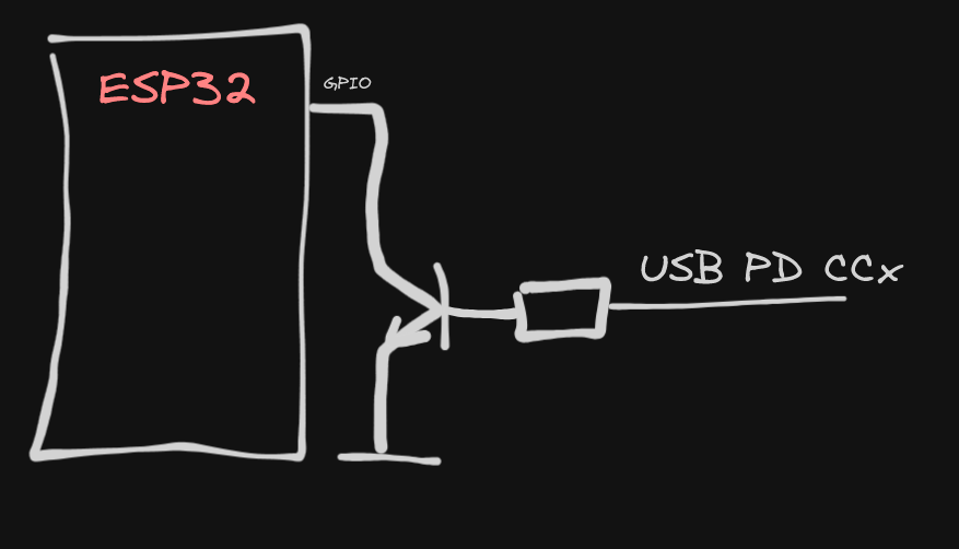
Basically I want this setup.
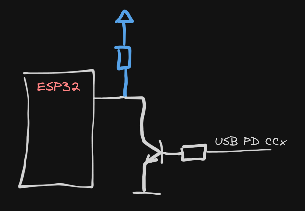
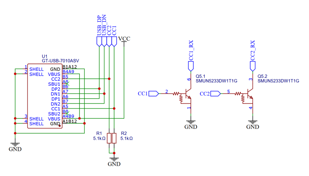
Checking all the available parts in my home lab, I stumbled upon the MUN5233DW, a dual NPN with already integrated base resistor in a conviniently small SOT-363 package. Perfect match. That 47k is not required, but should also not hurt. Great for the Rx part, maybe even for Tx, wel will see later.
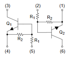
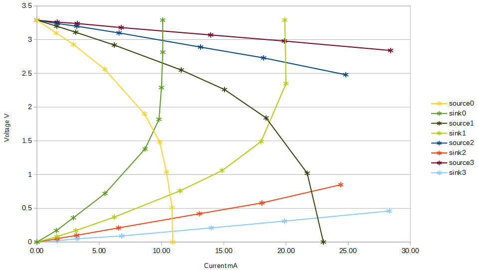
Now to reduce the BOM, I remove the blue pull up resistor and use the GPIO of the ESP32 with weak output drivers, sourcing 5mA according to spec and 10mA to measurements done by user Archibald on esp32.com. Here an image of his measurements. They show that the output current is limited by the output driver. So we save the pull up resistor.
So we end up with the Rx part to just drive the output GPIO low, which the input logic of that GPIO properly registers as low. Yes, this is legal, although it feels weird. We must however make sure that the sum of all driven outputs is – according to ESP32 specs – below 40mA.
This is the Rx part:
Transmission
Now when transmitting, there are some more issues than you would expect. First of all, we must make sure we drive the line to 0V and pull it back to ~1.2V with a frequency of 600kHz.
This is not as simple as it seems on the first look. If we just place a voltage divider, driving the line low happens via that lower resistor. And depending on the resistor value and pull ups on that line, the voltage drop may get quite high.
Thus the “low” voltage is not at 0V, but hundreds of mV, which makes detecting the bits unreliable for the other receiver.
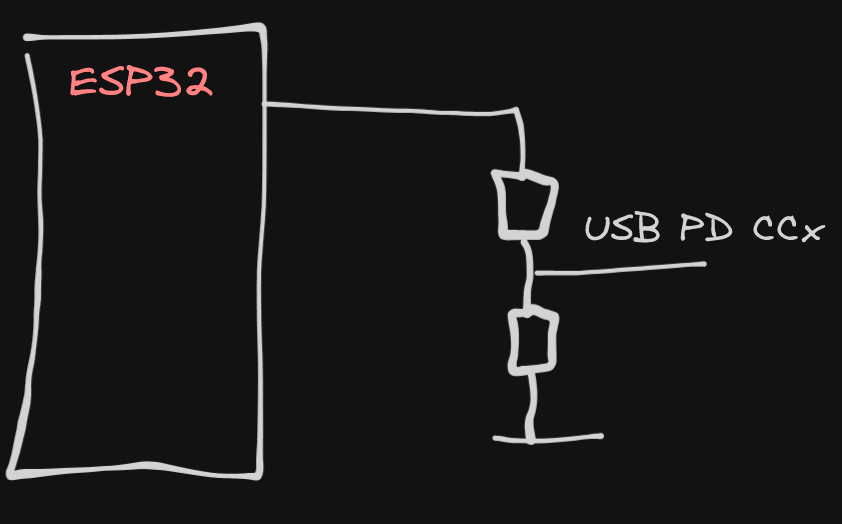
Another, better option is to use the GPIO as open drain switch, pulling the USB CC line low, which gets biased to 1.2V using a voltage divider.
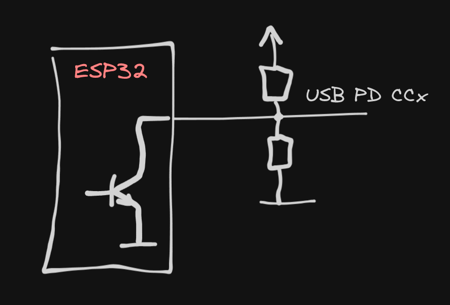
With that method we have – depending on the resistor values – a proper 1.2V high and proper 0V low signal. Unfortunately I don’t think that works, as per USB PD spec the power supply expects a 5.1k resistor “Rd” and when we have a resistor network driving the line all the time, that would confuse the power supply.
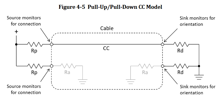
So the only simple options I see, are
- directly driving the CC line with GPIO to 3.3V
- driving the CC line with GPIO to 3.3V while having another GPIO weakly pull to ground, building a voltage divider
While the first option is very simple, it might trigger a “loss of 5.1k pulldown” and thus a PD disconnect when the voltage is too long, too close to 3.3V. (spoiler: it works just as fine)
So my primary approach is to build a configurable divider, pulling CC low with variable drive strengths. If you check the voltage/current diagram and search where lines are crossing, these are the voltage levels we can generate. The closest crossing between the plots are at 0.7V and 1.6V. Measuring them on a real PCB, shows they are more 0.8V and 1.7V, but thats also okay-ish. Both lie outside the specs, so I’d recommend 1.7V.
Signal Generation/Decoding
The signal is not just a simple serial protocol like you’d expect from an UART. It is manchester encoded with a zero encoded as “just change” and a one encoded with a double-change of the signal level. This is a common signal encoding scheme that helps with clock recovery and maintains a DC-free signal line.
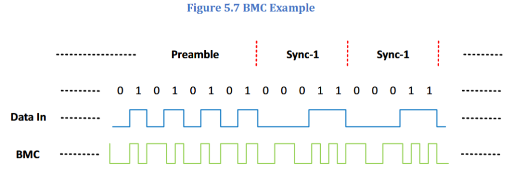

On top of the BMC encoding, there is a simple packet format, with a preamble, start symbols and a end-of-packet-marker. All well described in the USB spec and nothing of surprise.
Well, except the LSB first transmission, which – i dont know why – caused me a mixups a few times.
Okay, back to peripheral chosing. Instead of bitbanging, we again have two options here with the ESP32.
- we can use the I²S peripheral to constantly sample the CC line and manually (using the CPU) to recover the bits from the signal
- or we can use the wonderful RMT peripheral, which gives us a sequence of levels and their duration
As you already read from the list, I love the RMT peripheral and we will use it with some manual labor to generate and decode the manchester signal.
It would get a bit lengthy to describe exactly how to decode the signal, so I will keep it short.
Decoding
The ESP32-C3 supports the so called ping-pong-mode which fills the buffer in a circular manner and triggers an interrupt at a certain buffer position. This gives our code the chance to pick up the newly generated samples and process them continuously.
All this is already implemented in the ESP-IDF framework, so we just need to implement a CBR which conviniently has to process the supplied sample buffer.
Generation
Using the same peripheral we can generate the encoded signal with the same ease as when decoding.
PD protocol specialities
Lets better talk about the “not so obvious” things, that i’ve faced with that project.
There is only one headline for this:
Timing
First of all, every packet contains a CRC-32 which the receiver has to check and to acknowledge with a GoodCRC message. The receiver has a time window of less than a millisecond to respond with this message, else the sender will retransmit a few times.
While this is the first thing that I expected to get complicated, it turned out to work quite well. My approach was to configure the RMT driver to place code in IRAM. Unfortunately I could not trigger the RMT TX from IRAM. I got an abort trap which is a sign that the TX code is still in flash and from an IRAM ISR I cannot call flash code.
So I solved this by having a highest-priority task for tx confirmation that gets activated by the RX-ISR. With that approach I got a delay below 200us in a test setup just from “rx finished” to “toggle GPIO”.
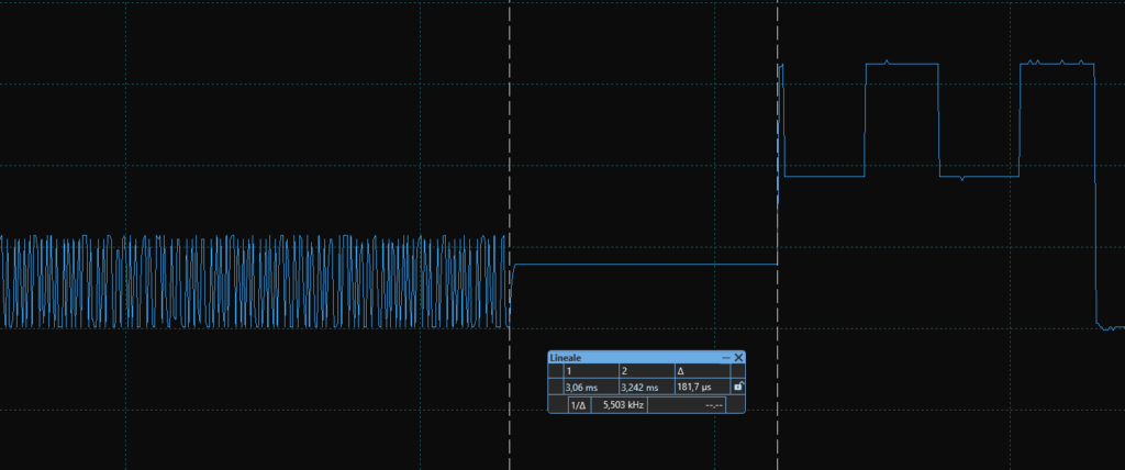
This is a good basis, processing the bits and calculating the checksum adds some more microseconds, but thats fine.
Another timing sensitive thing, which was not that obvious, cost me a whole night of debugging. Whenever the source announces its capabilities, the sink has to send another request as a response to that. If the sink doesn’t respond, the source sends a hard reset and unpowers VBUS.
This happened to me for hours. I received the capabilities report, requested a profile from it and the power supply accepted it. Then the source sent another (changed) capability report I didnt’t respond to and then the lights went out. My first thoughts were of course that I’ve messed up the GoodCRC or when playing around with voltage levels, but it was just the fact that the next capabilities report had an entry less and the supply wanted me to confirm it.
And why is it a timing issue? Even if you print out a few lines with ESP_LOGI, will delay the transmission of the request response so much, that the source will still reset the PD communication.
So I had to ensure that there is not just a “low latency” GoodCRC response, but also a low latency “protocol-handling-and-respond” path. By how much can the answer be delayed? Is it also a millisecond or longer? It’s longer, but i am not sure by how long. Did not find it in the specs yet, or have determined it experimentally. Right now the code works. It needs some more structuring and some features are missing.
So if you want to support, just contact me. You’ll find a way :)
Current state
It is still designed for a single CC line, but can be extended to handle both lines without much overhead. You can also save another GPIO by driving the CC line with its 3.3V directly.
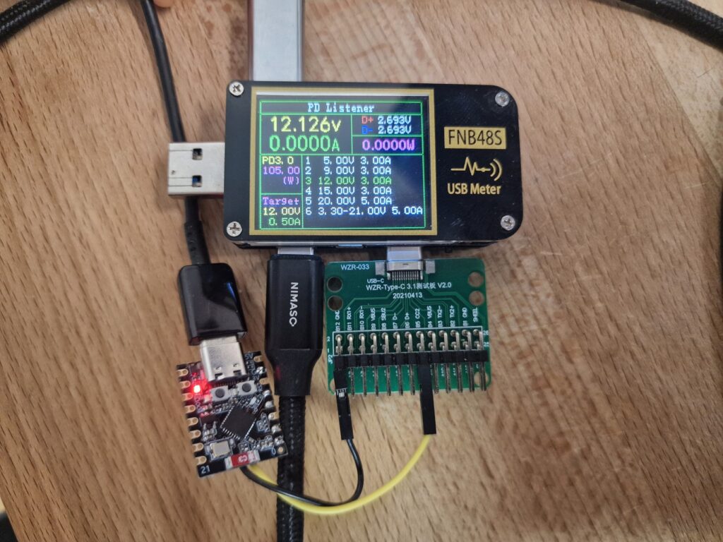
And how does my current test setup look like in a closer view? Forgive me the ugliness, I soldered around a few times and did some other tests with extra resistors and still use a GPIO to attach the 5.1k pulldown to make the source detect the sink.
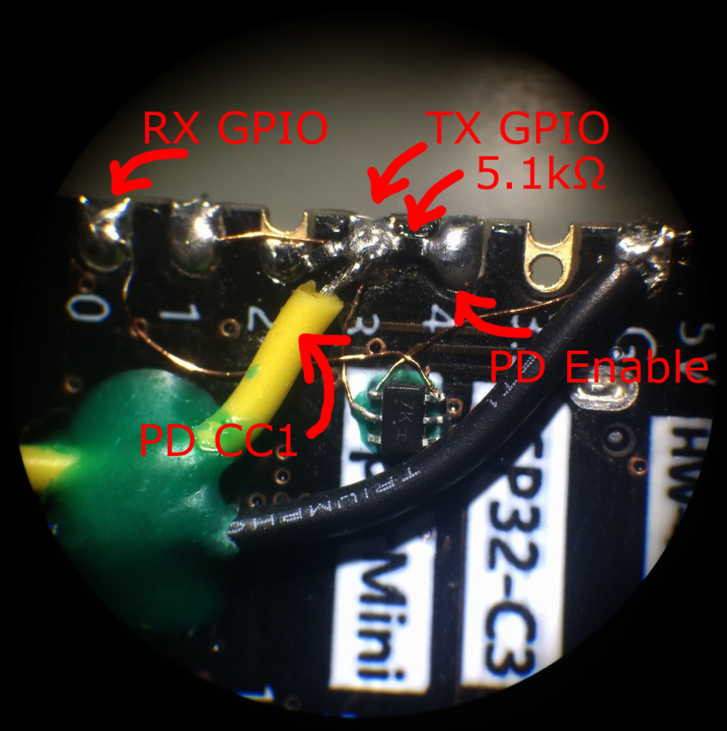
Basically you see the tiny SOT-363 transistor pulling the RX GPIO (0) to ground (top right, G pad) whenever the signal on CC1 (3) gets high. As written above, the CC1 can also weakly get pulled towards GND to form a voltage divider, this was done using another GPIO (1). Currently I am driving the full 3.3V on the PD line, which works just fine and makes this CC GPIO obsolete. Also ignore the resistor on GPIO2, which was just for testing around.
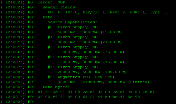
Here are some logs from the traffic my ESP32 sees on the PD bus. The first messages are the source enumerating which cable is present and then we got an announcement of the capabilities.
I (237544) PD: Target: SOP'
I (237544) PD: Header Fields
I (237544) PD: DO: 1, ID: 0, PPR/CP: 0, Rev: 2, PDR: 0, Type: 15
I (237544) PD: Data:
I (237544) PD: Vendor Message:
I (237554) PD: Vendor Message:
I (237554) PD: VDM Header 0xff00a001
I (237564) PD: SVID: 0xFF00
I (237564) PD: VDM Type: Structured
I (237574) PD: VDM Version: 1.0
I (237574) PD: Object Position: 0
I (237584) PD: Command Type: 0
I (237584) PD: Command: 1
I (237594) PD: Data bytes:
I (237594) PD: 8f 10 01 a0 00 ff a4 45 02 72

I (237604) PD: Target: SOP'
I (237604) PD: Header Fields
I (237604) PD: DO: 0, ID: 0, PPR/CP: 1, Rev: 0, PDR: 0, Type: 1
I (237614) PD: Control:
I (237614) PD: Good CRC
I (237624) PD: Data bytes:
I (237624) PD: 01 01 28 13 c5 2f
I (237634) PD: Target: SOP'
I (237634) PD: Header Fields
I (237634) PD: DO: 5, ID: 0, PPR/CP: 1, Rev: 2, PDR: 0, Type: 15
I (237644) PD: Data:
I (237644) PD: Vendor Message:
I (237654) PD: Vendor Message:
I (237654) PD: VDM Header 0xff00a041
I (237664) PD: SVID: 0xFF00
I (237664) PD: VDM Type: Structured
I (237674) PD: VDM Version: 1.0
I (237674) PD: Object Position: 0
I (237684) PD: Command Type: 1
I (237684) PD: Command: 1
I (237694) PD: Data #1: 0x18000000
I (237694) PD: Data #2: 0x00000000
I (237694) PD: Data #3: 0x00000000
I (237704) PD: Data #4: 0x00082042
I (237704) PD: Data bytes:
I (237714) PD: 8f 51 41 a0 00 ff 00 00 00 18 00 00 00 00 00 00
I (237714) PD: 00 00 42 20 08 00 5f 1e bc c0
I (237734) PD: Target: SOP'
I (237734) PD: Header Fields
I (237734) PD: DO: 0, ID: 0, PPR/CP: 0, Rev: 0, PDR: 0, Type: 1
I (237744) PD: Control:
I (237744) PD: Good CRC
I (237744) PD: Data bytes:
I (237754) PD: 01 00 be 23 c2 58I (237764) PD: Target: SOP
I (237764) PD: Header Fields
I (237764) PD: DO: 6, ID: 0, PPR/CP: 1, Rev: 2, PDR: 1, Type: 1
I (237774) PD: Data:
I (237774) PD: Source Capabilities:
I (237774) PD: #0: Fixed Supply PDO
I (237784) PD: 5000 mV, 3000 mA (15.00 W)
I (237784) PD: #1: Fixed Supply PDO
I (237794) PD: 9000 mV, 3000 mA (27.00 W)
I (237794) PD: #2: Fixed Supply PDO
I (237804) PD: 12000 mV, 3000 mA (36.00 W)
I (237804) PD: #3: Fixed Supply PDO
I (237814) PD: 15000 mV, 3000 mA (45.00 W)
I (237814) PD: #4: Fixed Supply PDO
I (237824) PD: 20000 mV, 5000 mA (100.00 W)
I (237824) PD: #5: Augmented PDO (SPR PPS)
I (237834) PD: 3300 mV - 21000 mV, 5000 mA (Limited)
I (237844) PD: Data bytes:
I (237844) PD: a1 61 2c 91 01 08 2c d1 02 00 2c c1 03 00 2c b1
I (237854) PD: 04 00 f4 41 06 00 64 21 a4 c9 be 41 6e 93
The code is published at Github and triggers the requested voltage, reporting back a max current you expect to draw. I tested it with a few supplies and power banks, giving consistently good results – delivering the requested voltage.
Here is a schematic of my Zigbee switch v2.0, which is not tested yet and contains CC1/CC2 support. As you can see, I dropped the approach with GPIOs pulling down the output voltage there, so driving the PD with 3.3V directly. Will test is and report back if it worked.
Update 09.01.2025
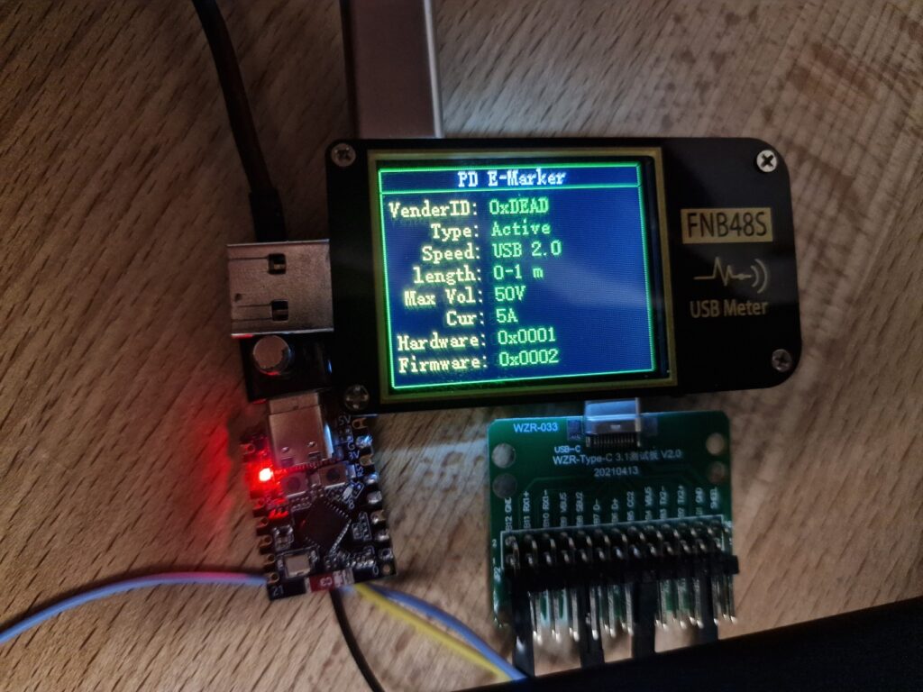
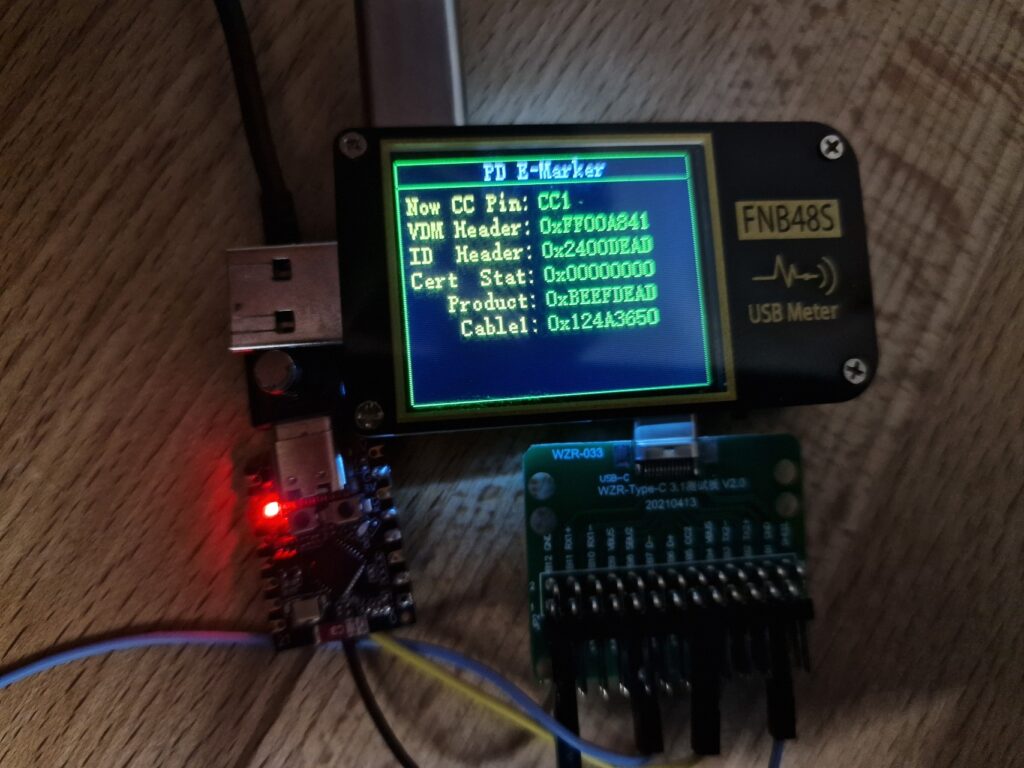
Due to a question on discord I peeked into the cable detection and ended up in implementing the VDM responses, a cable has to send. So now there is code to tell the supply that the device also contains a cable which is e.g. EPR capable with 50V/5A. Due to lack of a power supply I could not really test it, if that works. It seems that my code is maybe too slow and probably violating tVDMReceiverResponse (15ms) because the source did not accept my response to the VDM request.
However a PD tester successfully reports a cable with the definitions I want it to have. Guess it needs some more tweaking of the timings and such.
Update 10.01.2025
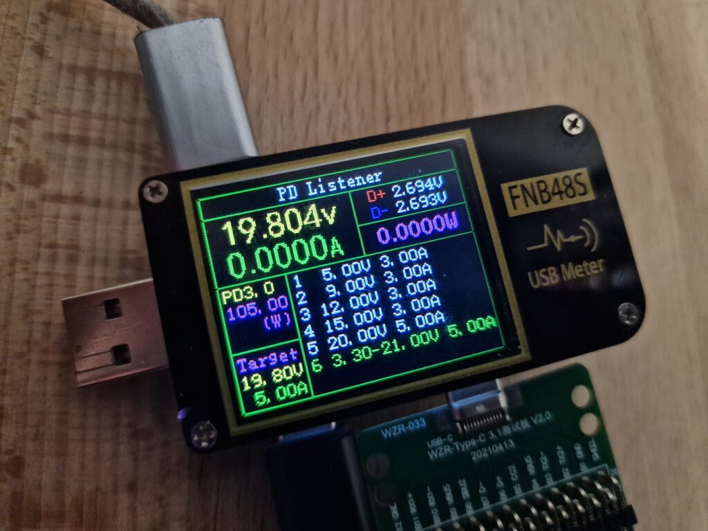
Another request to handle PPS was also implemented. So you can basically build your own power supply with an ESP32 and a PPS capable phone charger. The only thing you have to keep in mind is the fact that every 10 seconds the request must be sent again, else the supply enters some fallback mode without PPS. So now there is a periodic message that is being sent and not just a “fire and forget” startup code style.
Conclusion
Mission accomplished.
ESP32-C3 speaks USB PD with a single resistor and a SOT-363.
I already hear those comments saying “why don’t you just use a CH224K, its so cheap”.
My answer to them: You didnt get the point :)
This was again a funny and teaching journey in exploiting things and creating stuff that only few really need. Maybe it finds its way into some designs. If so, tell me.
